Continue to Site

Welcome to EDAboard.com

Welcome to our site! EDAboard.com is an international Electronics Discussion Forum focused on EDA software, circuits, schematics, books, theory, papers, asic, pld, 8051, DSP, Network, RF, Analog Design, PCB, Service Manuals... and a whole lot more! To participate you need to register. Registration is free. Click here to register now.

A new resonant DC-DC converter: Pe17 circuit

Atal

Junior Member level 2
Joined
Mar 25, 2018
Messages
24
Helped
0
Reputation
0
Reaction score
1
Trophy points
3
Activity points
131
I hereby present my newly invented resonant DC-DC converter circuit, named 'Pe17 circuit'.
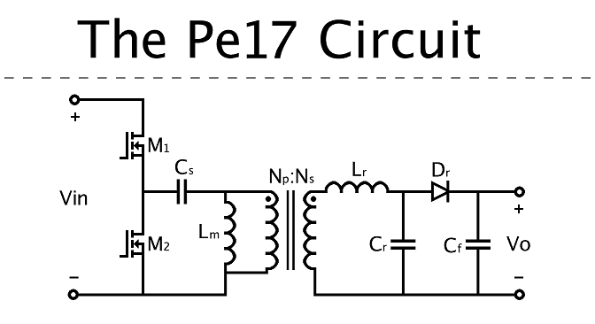
view1.PNG


view2.PNG


Features:
* Resonant half/full bridge inverter, utilizing ZVS operation.
* Constant frequency switching.
* Wide input/output voltage range operation capability, suitable also for EV battery chargers.
* Higher efficiency and power density.

Brief intro:

For more details, see US patent - US11139734:

Attached:
Presentation providing comparison between the Pe17 circuit and the LLC resonant circuit.
LTSpice simulation files for evaluation.
 

Attachments

  • Comparison of the Pe17 circuit and the LLC resonant circuit for power supply DC-DC conversion.pdf
    3.7 MB · Views: 214
  • simulation.zip
    70.2 KB · Views: 151
Great that you got there - but there is rarely anything new under the sun - see Russian and Japanese patents, it's common to put a diode across Cr ( this is very soft switched ) to limit the range of operation - which is often beneficial - and also an output choke before Cf

have you calc the AC ripple current in Cr - then tried to buy parts to match ?

An half bridge LLC with one more o/p diode achieves a similar result with far less components having to carry high ripple currents - although the "Pe17" has more degrees of control - i.e. can go to zero duty cycle = 0-full Vo and Io control.

look at light load / no load operation, look at V across Dr
 
Last edited:
Great that you got there - but there is rarely anything new under the sun - see Russian and Japanese patents, it's common to put a diode across Cr ( this is very soft switched ) to limit the range of operation - which is often beneficial - and also an output choke before Cf

have you calc the AC ripple current in Cr - then tried to buy parts to match ?

An half bridge LLC with one more o/p diode achieves a similar result with far less components having to carry high ripple currents - although the "Pe17" has more degrees of control - i.e. can go to zero duty cycle = 0-full Vo and Io control.

look at light load / no load operation, look at V across Dr

Thank you for your reply and comments.

I couldn't get anything informative from your suggestion to see 'Russian and Japanese patents'; every patent has a unique inventive concept, which cannot be hand-waved.

Please read first the attached presentation providing comparison between the Pe17 circuit and the LLC resonant circuit. It includes efficiency and loss breakdown, and p. 12 answers your question regarding the AC ripple current in the resonant capacitor. Further examination will lead you to the opposite conclusion regarding components count.

In the attached simulation files, specific components from various manufacturers are suggested (with text comments) for each power electronic element, including the resonant capacitor.

The brief intro also addresses your inquiry about light load/no load operation, and the reverse voltage across the rectifier.

[Moderator action: deleting comment about PM]
 
Last edited by a moderator:
Thank you for your interest.

The presentations I've provided are freely available for you and others to view, and obtain from them the values for the variables you're inquiring for the suggested specific design.

Please keep in mind that these are variables, as the specific design can be altered for the same application.
For example, the turns ratio of the transformer and the capacitance of the resonant capacitor can be reduced, while the circuit as a whole produces the same voltage gain and output power at the same switching frequency. Thus, a trade-off can be made between efficiency attributes such as current stress and/or voltage stress on the different components in the Pe17 circuit. Of course it is up to the design engineer to decide which design is optimal in consideration of parameters such as the output power, the output voltage, the input voltage and the operation frequency.

Further information can be found in US patent - US11139734.

Attached:
LTSpice simulation files for alternative design.
US patent - US11139734.
 

Attachments

  • simulation-alt.zip
    70.3 KB · Views: 126
  • US11139734.pdf
    884.2 KB · Views: 167
Last edited:
Atal,

I must say congratulations. It's always a thing of joy to conceive an idea and then convert it to reality. Sometimes when we see equations associated to an invention and it looks simple, we may undermine the work that the inventor put in before they could arrive at the conclusion of the 'simple' equation(s). Most times, the work that was put in would put some people to sleep.

I have mine too and they are yet to be patented.

Congratulations once again.
 
Thank you, Akanimo.

I wish you the best of luck in your endeavour.
I totally agree with your observation; in many ways being an inventor is under-appreciated. A famous guy named Nikola T. could also testify...

A further presentation providing comparison between the Pe17 circuit and the LLC circuit in EV battery charger application is underway.
 
Thanks, we need a "Buck converter" (2kW) to go after our PFC with 390Vout.....so that we can vary the input voltage to our 15kv output LLC converter.....the LLC is on open loop.
Can we use youir Pe17 to act as this "buck"?

..So it needs to Buck down from 390V, to any voltage between 390V and down to 100V....(2Kw)
(ie variable voltage output from 390V to 100V.....Vin = 390V)
 
A further presentation and simulation files regarding the Pe17 circuit in on-board EV battery charger are provided herein.
 

Attachments

  • Comparison of the Pe17 circuit and the LLC resonant circuit for DC-DC conversion in on-board E...pdf
    3.4 MB · Views: 137
  • simulation.zip
    40.6 KB · Views: 103
Last edited:
Thank you for your reply.

Soft switching is maintained regardless, but regulation with normal duty cycle control cannot be obtained at light loads for this specific design. Burst mode operation or charging pulses with rest periods are probably more appropriate and safer modes for EV batteries in those cases.
 
Last edited:
References related to the first presentation are provided.

1) Datasheet of a possible controller for the half bridge inverter:

2) Information regarding the ESR of C0G MLCC which are typically used as resonant capacitors:

3) Usage of film capacitors instead of elcaps as DC link capacitors:

4) Design guidlines for magnetic integration of resonant inductors in transformers:
 
Sorry to bump this, but it may be of interest in the discussion of new resonant converters...

Today i ran a Isolated resonant converter at 240VAC, 150W, 36vout. It had significant 100Hz ripple (~3Vpkpk) at vout due to only 560nF at the input Bus. "565k450N" (film cap)
Had 2mF at Vout.
It was able to switch right across most of the mains haversine.
There was no resonant cap on the primary side. Transformer had significant leakage L.
Single pri coil, single sec coil.
Neither end of the sec coil was connected to either neg or pos output terminals.....due to the series capacitors on the output.

Output was a bit unusual.

Output (sec) was kind of a full bridge arrangement.....2 bottom fets....2 top capacitors....and the Vout being literally the bridge. One fet "right way up"..other "other way up"

It had a totem pole of GaN FETs at pri..and two sync GaN FETs at sec. No heatsinks in sight. FETs all ran very cool. (didnt burn my finger one bit when i touched them after turning off).

Oh, and funny thing....there was a 33uF cap on the DC bus...but diode fed from the DC bus...so it couldnt be used by the lower fet to draw current from it for a power switching cycle....this cap was seen going up to near 500V when i took it up to 230W......The "diode" may have been a TVS....marked "QE1J\"

Transformer looked like PQ...27mm x 25mm x 21mm or so.

Anybody know the name of it?...or something similar?...unfortunately i cannot show it.
 
Last edited:
Just by way of illustration perhaps you can state the rms current in Cr, Lr, and Nsec for 500W, 12V out (41.7A out ) ... ?

In the alternative design, the current through the 247 nF resonant capacitor is 23.4 Arms.
This resonant capacitor can be comprised of 5 x 47 nF.
TDK's 47 nF capacitor has ESR of ~2.5mohm at 500 kHz:
product.tdk.com/en/system/files?file=dam/doc/product/capacitor/ceramic/mlcc/charasheet/cga5h2c0g1h473j115aa.pdf

Thus, the dissipation and temperature rise of each 47 nF is 55 mW and 21°C.
The total dissipation in the resonant capacitor would be 275 mW.

In the alternative design, the current through the secondary winding is 61.6 Arms, which is less compared with currents of 2 x 33.4 = 66.8 Arms in the LLC converter. Plus, the secondary current in the Pe17 circuit is nearly sinusoidal, whereas in the LLC converter, the secondary currents contain large portion of second order harmonics due to their half-sine waveshape.

fft-Pe17.PNG


fft-LLC.PNG
 
To illustrate the merit in having the DC-DC converter operating under wide input voltage range, take for example the be quiet! Dark Power 13 1000 W PSU -
hwbusters.com/psus/be-quiet-dark-power-13-1000w-psu-review/3

By letting the peak-to-peak ripple between 540 V and 380 V, the two 470 uF elcaps -
www.mouser.com/ProductDetail/United-ChemiCon/EKMZ421VSN471MR35S?qs=u4fy%2FsgLU9M6Zb6K%2FxQJ5A%3D%3D

can be replaced with a single 50 uF film capacitor -
www.mouser.com/ProductDetail/EPCOS-TDK/B32778Z8506K000?qs=RcG8xmE7yp0p3dwDjPgkuQ%3D%3D

thus saving ~13 $ and retaining almost the same volume density without considering durability, efficiency difference or complex inrush protection circuitry.

This of course requires the DC-DC converter to oparate under variable voltage gain. The following on-board charger datasheet reveals the excessive amount of elcaps being present just to maintain a fixed gain in the DC-DC stage -
assets.wolfspeed.com/uploads/2020/12/CRD-06600FF10N.pdf
 
Provided herein is a schematic diagram of the Pe17 circuit:
schematic.png

It features standby mode and burst mode operation under ZVS.

Further details will be provided soon.
 
The following simulation diagrams shows the output voltage, the current of the bottom half-bridge switch, the magnetization current, the current of one of the synchronous rectifiers, and the control voltage of the synchronous rectifiers.

0001.gif

Transition from 10% load operation to full load operation


0002.gif

Transition from full load operation to 10% load operation
 
Thank you for your comment.
Please see application note for Gan-based 300W LLC DC-DC converter which uses a current-mode controller - NCP13992


The output voltage settles approx. in 0.3 ms after the step-load - similar to that of the Pe17 circuit.

1.PNG
 
Last edited:

LaTeX Commands Quick-Menu:

Similar threads

Part and Inventory Search

Welcome to EDABoard.com

Sponsor

Back
Top